
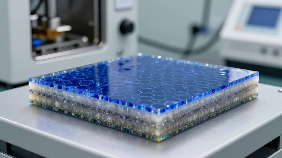
<p>Sapphire substrates are the most widely used substrate materials in the blue-green LED and Micro-LED epitaxy industries, with their quality directly determining the dislocation density of the epitaxial layers and the final device's light-emitting efficiency. Substrates are typically cut along the C-face (0001), and combined with patterned substrate technology to further enhance lattice matching and light extraction efficiency.</p><p>There are three key aspects of incoming material control: first, crystal orientation deviation—cutting angles for C-face substrates are generally maintained within ±0.1 degrees; excessive deviation can lead to noticeable step-flow growth non-uniformity in the epitaxial layer. Second, surface condition—epitaxy-grade substrates require atomic-level flatness, with roughness typically at the sub-nanometer level, and must be free from scratches, chipping, and particulate contamination. Third, geometric dimensions—including total thickness deviation, warp, and diameter tolerance—which directly affect uniform load-bearing in the epitaxy furnace and film thickness uniformity.</p><p>Before use, it is recommended to conduct batch-by-batch sampling inspections for birefringence and dislocation density, and verify batch consistency of the polishing process route (double-sided grinding followed by chemical mechanical polishing) to stabilize the epitaxy process window at the source and reduce inter-batch variations in wavelength uniformity and brightness distribution.</p>